- 您现在的位置:买卖IC网 > Sheet目录3882 > PIC18F4539-I/ML (Microchip Technology)IC MCU FLASH 12KX16 EE A/D 44QFN
PIC18FXX39
DS30485A-page 286
Preliminary
2002 Microchip Technology Inc.
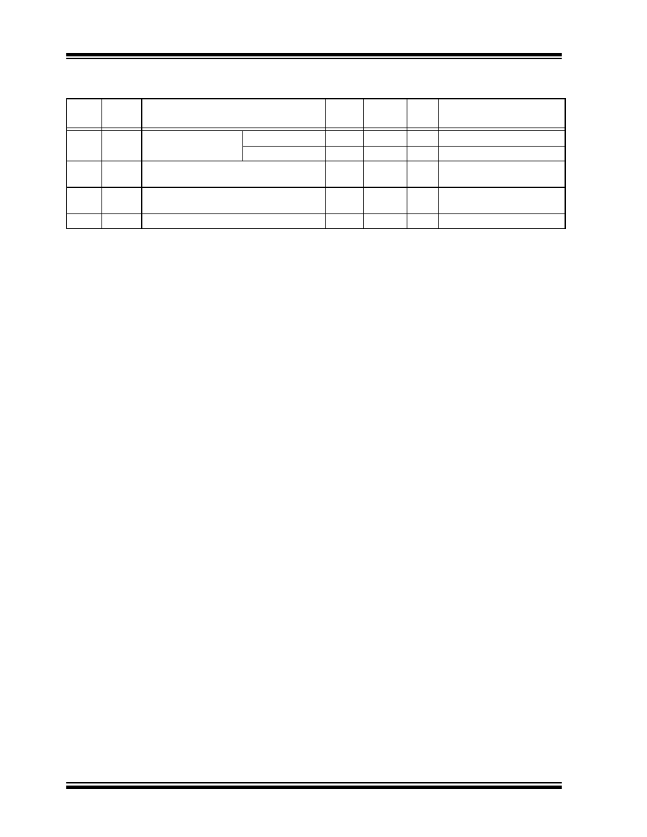
TABLE 23-22: A/D CONVERSION REQUIREMENTS
Param
No.
Symbol
Characteristic
Min
Max
Units
Conditions
130
TAD
A/D clock period
PIC18FXXXX
1.6
20(4)
sTOSC based
PIC18LFXXXX
2.0
6.0
s
A/D RC mode
131
TCNV
Conversion time
(not including acquisition time) (Note 1)
11
12
TAD
132
TACQ
Acquisition time (Note 2)
5
10
—
s
VREF = VDD = 5.0V
VREF = VDD = 2.5V
135
TSWC
Switching Time from convert
→ sample
—
(Note 3)
Note 1: ADRES register may be read on the following TCY cycle.
2: The time for the holding capacitor to acquire the “New” input voltage, when the new input value has not
changed by more than 1 LSB from the last sampled voltage. The source impedance (RS) on the input channels
is 50
. See Section 18.0 for more information on acquisition time consideration.
3: On the next Q4 cycle of the device clock.
4: The time of the A/D clock period is dependent on the device frequency and the TAD clock divider.
发布紧急采购,3分钟左右您将得到回复。
相关PDF资料
PIC18F4439-I/ML
IC MCU FLASH 6KX16 EE A/D 44QFN
PIC18F2439-I/SO
IC MCU FLASH 6KX16 EE A/D 28SOIC
PIC16F687-I/SO
IC PIC MCU FLASH 2KX14 20SOIC
PIC16F877AT-I/PTG
IC MCU FLASH 8KX14 W/AD 44 TQFP
PIC16F877A-I/LG
IC MCU FLASH 8KX14 W/AD 44PLCC
PIC12LC509AT-04I/MF
IC MCU OTP 1KX12 LV 8-DFN
PIC12C509AT-04I/MF
IC MCU OTP 1KX12 8-DFN
PIC24F08KL301-I/SS
IC MCU 16BIT 8KB FLASH 20-SSOP
相关代理商/技术参数
PIC18F4539-I/P
功能描述:8位微控制器 -MCU 24KB 1408 RAM 32 I/O RoHS:否 制造商:Silicon Labs 核心:8051 处理器系列:C8051F39x 数据总线宽度:8 bit 最大时钟频率:50 MHz 程序存储器大小:16 KB 数据 RAM 大小:1 KB 片上 ADC:Yes 工作电源电压:1.8 V to 3.6 V 工作温度范围:- 40 C to + 105 C 封装 / 箱体:QFN-20 安装风格:SMD/SMT
PIC18F4539-I/P
制造商:Microchip Technology Inc 功能描述:IC 8BIT FLASH MCU 18F4539 DIP40
PIC18F4539-I/PT
功能描述:8位微控制器 -MCU 24KB 1408 RAM 32 I/O RoHS:否 制造商:Silicon Labs 核心:8051 处理器系列:C8051F39x 数据总线宽度:8 bit 最大时钟频率:50 MHz 程序存储器大小:16 KB 数据 RAM 大小:1 KB 片上 ADC:Yes 工作电源电压:1.8 V to 3.6 V 工作温度范围:- 40 C to + 105 C 封装 / 箱体:QFN-20 安装风格:SMD/SMT
PIC18F4539IPT
制造商:MICRO CHIP 功能描述:NEW
PIC18F4539T-E/ML
功能描述:8位微控制器 -MCU 24KB 1408 RAM 32 I/O RoHS:否 制造商:Silicon Labs 核心:8051 处理器系列:C8051F39x 数据总线宽度:8 bit 最大时钟频率:50 MHz 程序存储器大小:16 KB 数据 RAM 大小:1 KB 片上 ADC:Yes 工作电源电压:1.8 V to 3.6 V 工作温度范围:- 40 C to + 105 C 封装 / 箱体:QFN-20 安装风格:SMD/SMT
PIC18F4539T-E/PT
功能描述:8位微控制器 -MCU 24KB 1408 RAM 32 I/O RoHS:否 制造商:Silicon Labs 核心:8051 处理器系列:C8051F39x 数据总线宽度:8 bit 最大时钟频率:50 MHz 程序存储器大小:16 KB 数据 RAM 大小:1 KB 片上 ADC:Yes 工作电源电压:1.8 V to 3.6 V 工作温度范围:- 40 C to + 105 C 封装 / 箱体:QFN-20 安装风格:SMD/SMT
PIC18F4539T-I/ML
功能描述:8位微控制器 -MCU 24KB 1408 RAM 32 I/O RoHS:否 制造商:Silicon Labs 核心:8051 处理器系列:C8051F39x 数据总线宽度:8 bit 最大时钟频率:50 MHz 程序存储器大小:16 KB 数据 RAM 大小:1 KB 片上 ADC:Yes 工作电源电压:1.8 V to 3.6 V 工作温度范围:- 40 C to + 105 C 封装 / 箱体:QFN-20 安装风格:SMD/SMT
PIC18F4539T-I/PT
功能描述:8位微控制器 -MCU 24KB 1408 RAM 32 I/O RoHS:否 制造商:Silicon Labs 核心:8051 处理器系列:C8051F39x 数据总线宽度:8 bit 最大时钟频率:50 MHz 程序存储器大小:16 KB 数据 RAM 大小:1 KB 片上 ADC:Yes 工作电源电压:1.8 V to 3.6 V 工作温度范围:- 40 C to + 105 C 封装 / 箱体:QFN-20 安装风格:SMD/SMT